3D-Printed Fiber-to-Chip Couplers for Integrated Photonics
Photonic integrated circuits are a key technology to reduce size and costs in complex optical systems, particularly thanks to miniaturization of photonic components. The applications of integrated photonics ranges from data and telecommunications to autonomous driving by means of LIDAR systems and mobile sensing devices in the medical field. Photonic integrated circuits also rely on key interfaces to connect, for example, chips to fibers, increasing integration and functionality. The fabrication of such interfaces can be challenging and involves difficulties in alignment, efficiency, and bandwidth. To tackle these issues, scientists present a new concept of broadband fiber-to-chip coupling based on 3D nanostructures fabricated by means of Nanoscribe’s 3D printers.
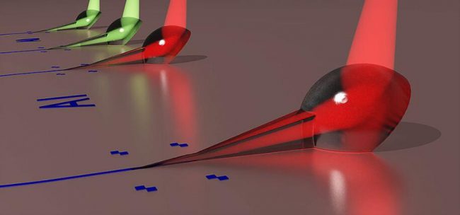 Rendering of freeform 3D couplers attached to a nanophotonic circuit for fiber-to-chip coupling. Image: W. Hartmann, H. Gehring, W. Pernice et al., University of Münster
![]() 3D-printed couplers connect chips to fibers
3D-printed couplers connect chips to fibers
A multidisciplinary team from the University of Münster – Institute of Physics, the CeNTech-Center for Nanotechnology together with the Max Born Institute and the Humboldt University of Berlin develop a concept of 3D polymer couplers that connect chips to fibers. These 3D couplers operate based on total internal reflection and are 3D-printed directly on photonic integrated circuits. The novel approach is designed for low-loss and broadband fiber-to-chip coupling in the visible wavelength range. The design combines a mode converter, a total reflection plane, and a sphere that works as a lens focusing the beam onto the fiber facet. The results of this investigation demonstrate a scalable coupling concept realized by means of 3D Microfabrication.
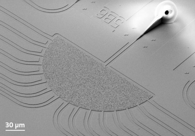 Spectroscopic device with a 3D-printed freeform coupler on total internal reflection for broadband fiber-to-chip coupling. Image: W. Hartmann, H. Gehring, W. Pernice et al., University of Münster
![]() 3D Microfabrication enables photonic packaging
3D Microfabrication enables photonic packaging
Several steps are needed in conventional methods to assemble various photonic and optical components on one microchip. Using 3D Microfabrication, high-precision and even freeform microparts can be easily printed on a photonic integrated circuit. The printing process does not require any further assembly, alignment, pick and place or fixing steps. Thus, the 3D printing can save equipment costs and time in photonic packaging.
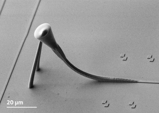 SEM of a freeform 3D fiber-to-chip coupler printed by means of Nanoscribe’s Photonic Professional GT system and connected to a silicon nitride waveguide. Image: H. Gehring, W. Hartmann, W. Pernice et al., University of Münster
![]() Nanoscribe joins research projects on integrated photonics
Nanoscribe joins research projects on integrated photonics
With its 3D Microfabrication know-how Nanoscribe participates in various research projects to develop novel technologies based on integrated photonics. For example, in the MiLiQuant research project, Nanoscribe works together with partners in science and industry to develop miniaturized, frequency- and power-stable diode lasers. The project aims to produce suitable radiation sources for industrial applications in medical diagnostics, sensors for autonomous driving and quantum-based imaging methods. Moreover, earlier this year, Nanoscribe joined the EU-funded research project HandheldOCT. Scientists and engineers from universities, research institutes and companies work together in this project to develop a handheld imaging device for mobile eye examination. In this way, Optical Coherence Tomography (OCT) is being expanded from stationary clinical use to a broader, mobile use in ophthalmologic care.
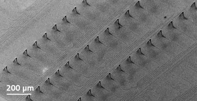 SEM of a photonic chip with several devices illustrating scalable fabrication of hybrid 3D-planar photonic circuits. Image: W. Hartmann, H. Gehring, W. Pernice et al., University of Münster
Source: Nanoscribe



Recent Comments